Our Technology
The highest image quality at the lowest practical X-ray dose is the challenge for all X-ray detectors, in all use cases. Perovskite-based detectors have a unique set of attributes that allow them to out perform existing photon-counting and scintillator based detectors. Additionally, their solution-based manufacturing process makes them quicker and more cost-effective to manufacture at scale, improving supply chain resilience.


![]()
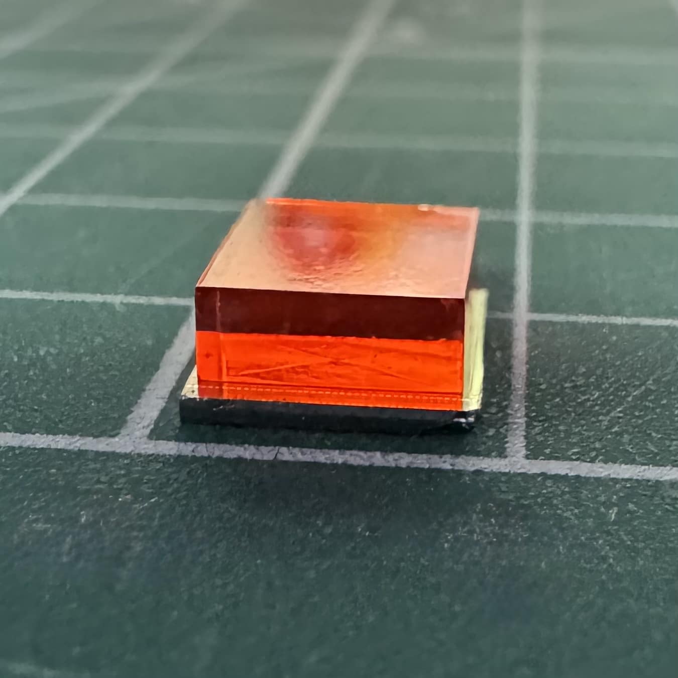
Our second-generation photon-counting X-ray detector (PRISM-X) harnesses the power of perovskite semiconductor materials to further improve imaging performance. Perovskites combine excellent X-ray attenuation with precise charge transport, enabling unprecedented spectral resolution and sensitivity.
With this technology, our detectors will deliver clearer, faster, and more informative images at lower X-ray doses, uncovering subtle contrast and fine detail that conventional detectors may miss. Their low-temperature, scalable manufacturing also paves the way for cost-effective imaging systems across industrial imaging, security baggage and parcel scanning, and medical CT and X-ray applications.


Perovskite
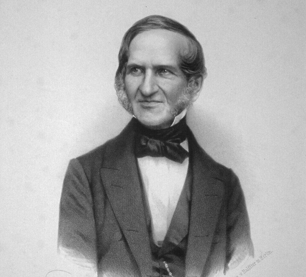
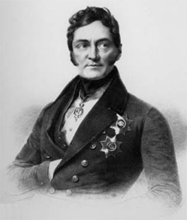
Perovskite is a term that describes a broad family of crystals built from repeatable, cuboidal structures that are similar to calcium titanate. Discovered by Gustav Rose (left image) in the Ural mountains in 1839, these crystals were named after Lev Perovski (right image), a Russian nobleman and mineralologist. The structure of perovskite was first described by Victor Goldschmidt, a Swiss-born, Norwegian geochemist in 1926, who is considered to be the founder of modern inorganic crystal chemistry.
More recently, Prof. Sam Stranks (University of Cambridge and Co-founder & CSO, Clarity Sensors) has played a pioneering role in the development and understanding of halide perovskite semiconductors, which are used in solar cells, LEDs, and X-ray detectors. His research has developed some of the key perovskite materials, uncovered how charge carriers behave and recombine in perovskites, identified sources of efficiency losses, and revealed how these materials degrade over time. Using advanced material characterisation techniques like optical spectroscopy and nanoscale microscopy, Stranks’ work has guided the design of longer-lasting, high-performance perovskite devices such as x-ray detectors and solar cells.
Image credit (left image): Rudolph Hoffmann, Public domain, via Wikimedia Commons
Image credit (right image): Friedrich Jentzen, Public domain, via Wikimedia Commons


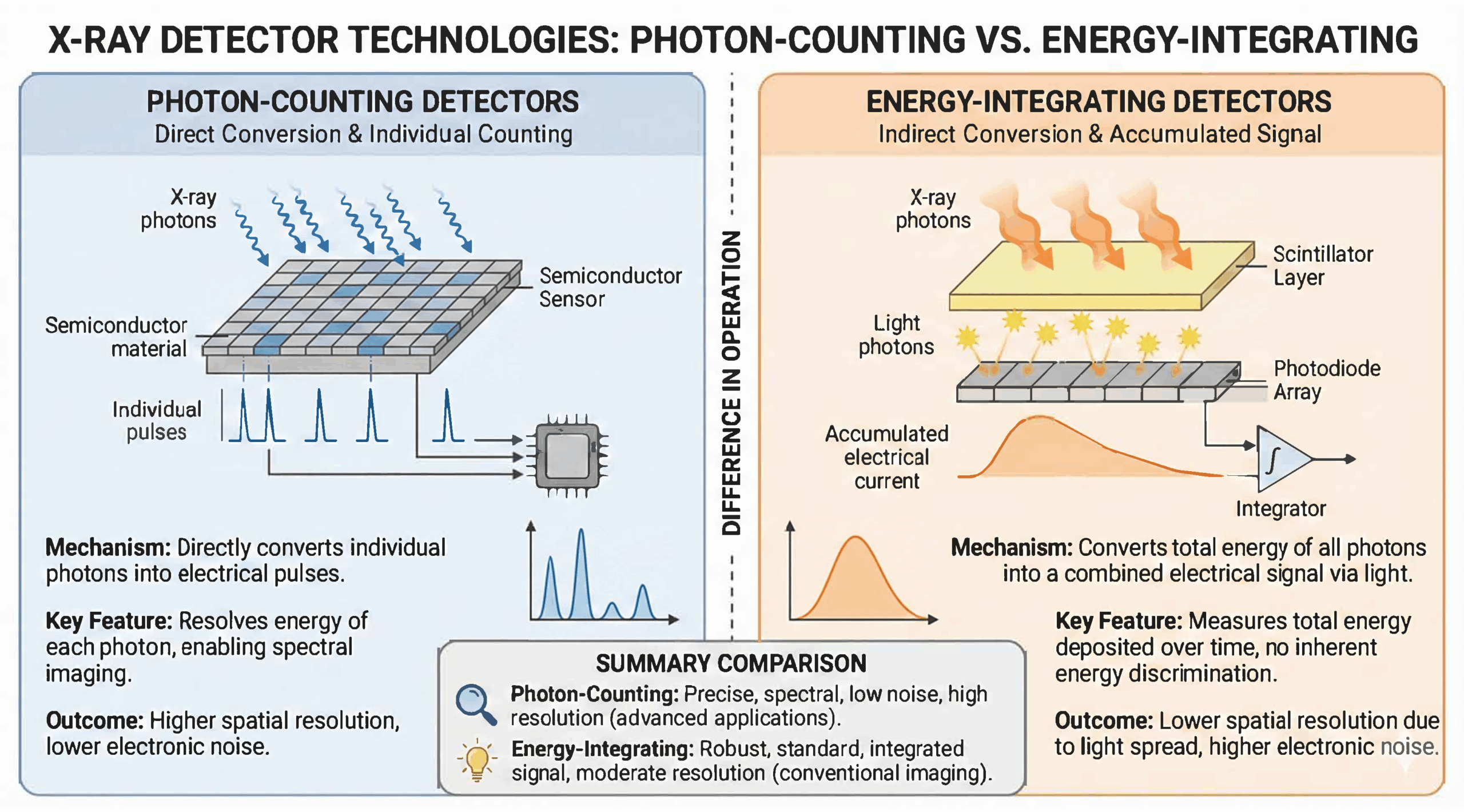
Photon Counting
Existing CT scanner detector technology converts the incident photons into light using a technique called scintillation. The photon travels through the tissue/material/sample and hits a scintillator crystal in the detector causing it to release flashes of visible light. The number of light photons released is proportional to the energy of the incident X-ray. The light photons are converted to an electrical signal using a photodiode which is attached to the scintillator crystal. The signals are sent to a computer to be reconstructed into a digital image of the tissue/material/sample.
Photon counting detectors are semiconductor crystals and are much more efficient as they directly convert the incident X-ray photons into electrical charges. The charges are separated by biasing the crystal with a cathode on the top of the crystal and an anode on the bottom, which is pixelated. The pixels count the number of photons and register their energy level. This additional data, when converted into a digital image, makes photon counting images much clearer. Noise levels in photon-counting detectors are extremely low – they are often called ‘noiseless images’ which additionally improves image resolution. The energy level information captured means that images always have spectral information i.e. they can be coloured. With a very low noise level every photon can be counted meaning that images are intrinsically higher in resolution compared to existing detectors which miss lower energy photons as they are in the ‘noise’.